|
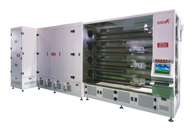
主要用于在低压环境下通过化学反应在晶圆表面沉积高质量薄膜,可沉积多晶硅(Poly-Si)、氮化硅(Si3N4)薄膜、氧化硅(SiO2)薄膜、BPSG薄膜、LTO薄膜 、HTO薄膜 、SIPOS薄膜、 BSG薄膜、 PSG薄膜等工艺。 It is mainly used to deposit high - quality thin films on the wafer surface through chemical reactions in a low - pressure environment. It can be used in processes such as depositing polysilicon (Poly-Si), silicon nitride (Si3N4) thin films, silicon oxide (SiO2) thin films, BPSG thin films, LTO thin films, HTO thin films, SIPOS thin films, BSG thin films, and PSG thin films. |
|
|
核心技术优势:Core technological advantages 高质量薄膜:High-quality thin films ◆ 低压环境(100-300 mtorr)减少气相反应,提升薄膜致密性、均匀性(厚度均匀性可达±1%以内) ◆ The low-pressure environment (100 - 300 mtorr) reduces gas-phase reactions, enhancing The compactness and uniformity of the thin films (the thickness uniformity can reach within ±1%). 优异阶梯覆盖能力:Excellent step coverage ability ◆ 适合高深宽比结构(如沟槽、孔洞)的均匀镀膜,避免边缘效应 ◆ It is suitable for uniform coating on structures with high aspect ratios (such as trenches and holes), avoiding edge effects. 材料适应性广Wide material adaptability ◆ 支持多种材料沉积(如硅片、玻璃、陶瓷、金属衬底等),工艺参数灵活可调。 ◆ It supports the deposition of various materials (such as silicon wafers, glass, cerami- cs, metal substrates, etc.), and the process parameters can be flexibly adjusted. 全自动化控制:Full Automation Control ◆ 集成了 SECS/GEM 标准通信接口,可无缝对接工厂自动化系统,实现设备状态实时监控、远 程参数调控以及生产数据的高效交互,为智能制造提供坚实保障。 ◆ SECS/GEM Integration: Equipped with a standard SECS/GEM communication interfa- ce, it can seamlessly connect to the factory automation system, enabling real - time monitoring of equipment status, remote parameter adjustment, and efficient exchange of production data, thus providing a solid foundation for intelligent manufacturing. |
|
|
主要参数: ◆ 适用硅片尺寸: 4-8英寸(兼容性设计) ◆ 温度均匀性≤±0.5℃(600-1200℃) ◆ 温度稳定性≤±0.5℃/24h(600℃) ◆ 工作压力: 100-300 mtorr ◆ 极限压力: 3 mtorr ◆ 漏率: 1mtorr/min ◆ 沉积速率: 1-15 nm/min(视材料与工艺条件) ◆ 薄膜均匀性: 片内/片间/批间均匀性±1% ◆ 非晶硅/多晶硅(poly)厚度均匀性:片内/片间/批次间≤ 1% ◆ D- Poly厚度均匀性: 片内/片间/批次间≤ 1.5% ◆ LTO厚度均匀性: 片内/片间/批次间≤ 2% ◆ TEOS厚度均匀性: 片内/片间/批次间≤1% ◆ Si₃N₄厚度均匀性: 片内/片间/批次间≤1% ◆ BPSG 厚度均匀性: 片内/片间/批次间≤2% ◆ SIPOS厚度均匀性: 片内/片间/批次间≤ 2% ◆ PSG厚度均匀性: 片内/片间/批次间≤2% ◆ THK氮氧化硅工艺(SiON)均匀性:片内/片间/批间/均匀性≤±2%(1000/5000 Å) ◆ 传送颗粒污染≤10ea(≥0.3μm) ◆ 工艺颗粒 污染≤20ea(≥0.3μm) ◆ 金属离子污染≤5e10(atom/cm 2) ◆ 气体系统: 高精度质量流量计(MFC)控制反应气体,尾气处理系统(Scrubber)集成 |
Main Parameters ◆ Applicable Wafer Size: 4 - 8 inches (with compatibility design). ◆ Temperature Uniformity: ≤±0.5℃ (600-1200℃) ◆ Temperature Stability: ≤±0.5℃/24h (at 600℃) ◆ Working pressure: 100 - 300 mtorr ◆ Ultimate pressure: 3 mtorr ◆ Leak rate: 1 mtorr/min ◆ Deposition rate: 1-15 nm/min (depending on materials and process conditions) ◆ Thin - film uniformity: Intra-wafer/inter-wafer/inter-batch uniformity within ±1% ◆ Amorphous Silicon / Polycrystalline Silicon (poly) Thickness Uniformity: Within-wafer / Wafer-to-wafer / Lot-to-lot ≤ 1% ◆ D-Poly Thickness Uniformity: Within-wafer / Wafer-to-wafer / Batch-to-batch ≤ 1.5% ◆ LTO Thickness Uniformity: Within-wafer / Wafer-to-wafer / Batch-to-batch ≤ 2% ◆ TEOS Thickness Uniformity: Within-wafer / Wafer-to-wafer / Batch-to-batch ≤ 1% ◆ Si₃N₄ Thickness Uniformity: Within-wafer / Wafer-to-wafer / Batch-to-batch ≤ 1% ◆ BPSG Thickness Uniformity: Within-wafer / Wafer-to-wafer / Batch-to-batch ≤ 2% ◆ SIPOS Thickness Uniformity: Within-wafer / Wafer-to-wafer / Batch-to-batch ≤ 2% ◆ PSG Thickness Uniformity: Within-wafer / Wafer-to-wafer / Batch-to-batch ≤ 2% ◆ THK Silicon Oxynitride (SiON) Process Uniformity: Within-wafer / Wafer-to-wafer / Batch-to-batch uniformity ≤ ±2% (at 1000/5000 Å) ◆ Transfer Particle Contamination: ≤10 ea (≥0.3μm) ◆ Process Particle Contamination: ≤20 ea (≥0.3μm) ◆ Metal Ion Contamination: ≤5e10 atoms/cm² ◆ Gas system: The reaction gases are controlled by high -precision mass flow controllers (MFCs), and an exhaust gas treatment system (Scrubber) is integrated. |

